
Silicon heterojunction cells (HET): a-Si:H/c-Si
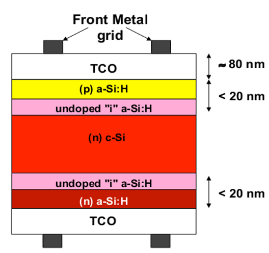
Silicon heterojunction cells (brand name HIT for "Heterojunction with In- trinsic Thin film") combining amorphous hydrogenated silicon layers (a-Si:H) with crystalline silicon substrates (c-Si) (see Fig. 1) are among the most efficient in silicon technology. GeePs has been studying this heterojunction for several years, and in particular the electrical and electronic properties (bending and energy band gap) of the a-Si:H/c-Si heterointerface by (photo)-electrical and transport measurements, often coupled with analytical calculations and numerical modelling [1]. A highlight is the demonstration of an inversion layer at the (p) a-Si:H/(n) c-Si interface by planar conductance measurements [1], capacitance measurements [2, 3] and conductive tip AFM (C-AFM) measurements [4].
 |
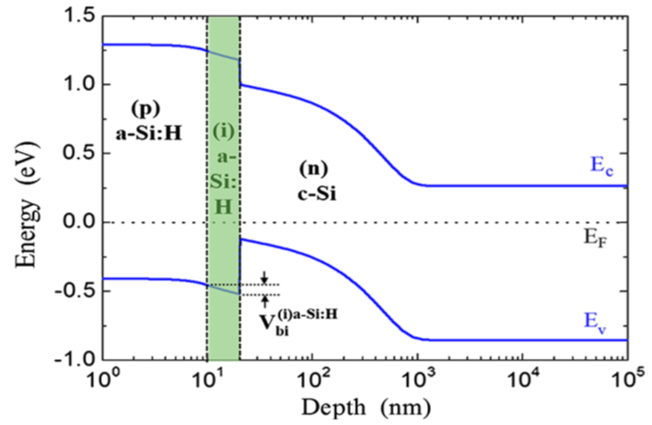 |
| Figure 1: Simplified diagram of a silicon heterojunction photovoltaic cell and its energy band diagram (semi-log scale) | |
The very good conversion properties of these cells depend in particular on the quality of the a-Si:H/c-Si interface. Indeed, this interface is characterised by the presence of a thin nanometric layer of intrinsic hydrogenated amorphous silicon (i) a-Si:H, called buffer, between the doped layer a-Si:H and the c-Si substrate. It should be noted that this hetero-interface has been the subject of many studies [6-10] which allowed us, among other things, to evaluate the B-band radiative recombination coefficient of crystalline silicon at low temperature (from 77 K to 20 K) for which no data was available to date [6].
A more recent study carried out on variable thicknesses of the buffer layer, (i) a-Si:H, has illustrated the impact of this thickness on the band curvature at the interface and more concretely on the concentration of minority carriers in the inversion layer. The planar conductance measurement applied to these different samples shows that it is directly linked to the conductance of the inversion channel (lateral hole current) present on the c-Si surface. These results are corroborated by 1D analytical calculations of the conductance in the inversion channel and 2D numerical simulations (TCAD-Silvaco) [9] presented in Fig. 2 [9]. Combining the experimental results with the 2D numerical modelling, it is further shown that the concentration of dangling bond defects, NDB, increases strongly with decreasing buffer layer thickness (see Fig. 3).
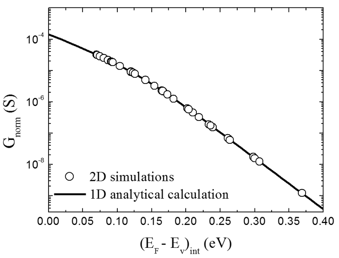 |
| Figure 2: Variation of conductance as a function of (EF-EV)int the distance between the Fermi level position and the conduction band on the c-Si surface. Extracted from Ref [9]. |
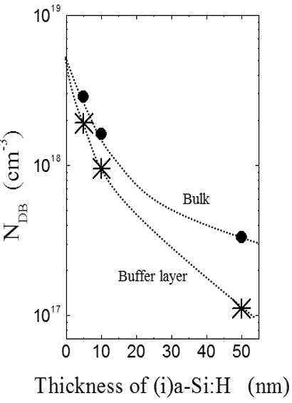 |
| Figure 3: Extracted deep defect density as a function of layer thickness (i). Extracted from Ref [9]. |
Another approach to studying the a-Si:H/c-Si hetero-interface was to apply the modulated photocurrent technique (MPC) which allowed the density of state at the interface, Dit, to be estimated as well as the carrier lifetime. The ability to combine MPC and MPL (modulated photoluminescence) at the same sample location shows that the Dit estimates are in agreement, and conversely reveals a discrepancy with respect to the carrier characteristic times. MPL is indeed directly sensitive to the effective time of the minority carriers in the absorber, whereas the MPC technique is sensitive to the inversion zone near the interface where the carriers are of the majority type [12].
Références
[1] J.-P. Kleider et al., Phys. Status Solidi A 2019, 1800877 (2019) ; DOI : 10.1002/pssa.201800877 ; hal-02308332 (https://hal.archives-ouvertes.fr/hal-02308332/)
[2] O. Maslova et al., Canadian Journal of Physics 92, 690-695 (2014) ; DOI : 10.1139/cjp-2013-0544 ; hal-01099596 (https://hal.archives-ouvertes.fr/hal-01099596/)
[3] O. Maslova et al., Journal of Applied Physics 118, 114507 (2015) ; 10.1063/1.4931150 ; hal-01310865 (https://hal-centralesupelec.archives-ouvertes.fr/hal-01310865)
[4] J.-P. Kleider et al. , Nanoscale Res. Lett. 6, 152 (2011) ; DOI : 10.1186/1556-276X-6-152 ; hal-00641696v1 (https://hal-centralesupelec.archives-ouvertes.fr/SUP_SCM/hal-00641696v1)
[5] These Ming Xu, Techniques de Photoluminescence pour l'étude des Interfaces Photovoltaïques (2016), tel-01319898, version 1 (https://tel.archives-ouvertes.fr/tel-01319898)
[6] R. Bruggemann et al., Phys. Status Solidi RRL 11, 1700066 (2017) ; DOI : 10.1002/pssr.201700066 ; hal-01631792 (https://hal.archives-ouvertes.fr/hal-01631792/)
[7] Thèse David Réaux, Cellules photovoltaïques à hétérojonctions de silicium (a-Si˸H/c-Si) : modélisation des défauts et de la recombinaison à l'interface (2017),
[8] D. Reaux et al, Energy Procedia 77, 153 (2015) ; DOI : 10.1016/j.egypro.2015.07.023 ; hal-01188802v1 (https://hal.inria.fr/PHEMADIC/hal-01188802v1) ; tel-01613084, version 1 (https://tel.archives-ouvertes.fr/tel-01613084)
[9] A. Levtchenko et al, Phys. Status Solidi RRL 13, 1900411 (2019) ; DOI : 10.1002/pssr.201900411 ; hal-02301811 (https://hal.archives-ouvertes.fr/hal-02301811)
[10] R. Varache et al. Journal of Applied Physics 112, 123717 (2012) ; DOI : 10.1063/1.4769736 ; hal-00778961 (https://hal-supelec.archives-ouvertes.fr/hal-00778961)
[11] S. Le Gall et al, 37th European Photovoltaic Solar Energy Conference and Exhibition (EU PVSEC 2020), hal-02946579 (https://hal.archives-ouvertes.fr/hal-02946579) et article en préparation (2021)
[12] These Alexandra Levtchenko, Étude de dispositifs photovoltaïques à hétérojonctions a-Si˸H/c-Si : caractérisations vs. simulations en régime modulé de structures planaires et modélisations optoélectroniques de nanofils à structure radiale (2019) ; tel-02068957, version 1 (https://tel.archives-ouvertes.fr/tel-02068957)