
Multi-junction structures
The most efficient solar cells to date are the so-called multi-junction structures. They consist of a stack of solar cells with decreasing absorption thresholds (optical band gap). The largest optical band gap is at the front.
In this multi-junction stack, the most energetic light is absorbed by the first "large gap" cell at the front, and the least energetic by the cell with the smallest gap at the back. This reduces the so-called thermalization losses, and allows higher conversion efficiencies, and therefore much higher electrical power, to be achieved. The interconnection of the multi-junction cell can be realised in different configurations. In the so-called two-terminal configuration (2T, cells connected in series) the current between the cells must be constant. This is a conceptually simple version, but technically difficult because of the current continuity, which also requires a tunnel junction between the cells. The three-terminal (3T) and four-terminal (4T) configurations minimise this constraint, at the cost of more complex connectivity. Figures 1a and 1b
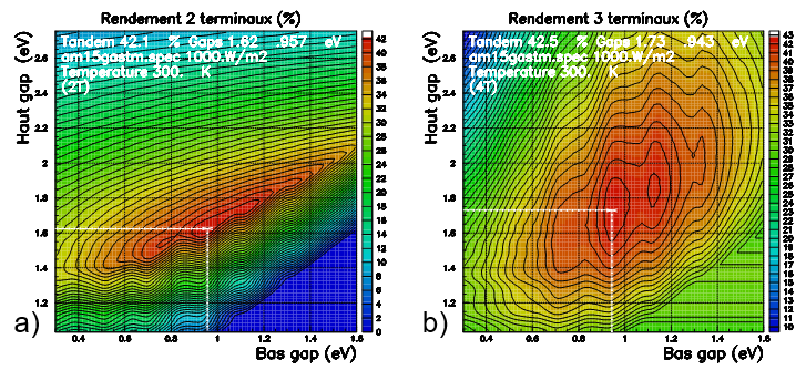 |
| Figure 1: Efficiency (without incident spectrum concentration) of two-subcell tandem multijunction cells as a function of high and low gaps of (a) two-terminal series subcells showing constant series current constraint and (b) three-terminal tandems where the subcells are independent and without series current constraints. |
The record multijunctions now achieve more than 45% efficiency under concentration (Green et al., Prog Photovolt Res Appl. 2020;28:629-638, http://dx.doi.org/10.1002/pip.3303).
On the other hand, the efficiency obtained from Si cells is close to 27%, which approaches the fundamental limit for this material of about 29%. The most promising route to increase the efficiency of Si-based cells is therefore new structures, with multijunction structures in the lead.
This research area is articulated on the axis of the study of new materials, in connection with their growth and characterisation, and on the axis of the development of classical and innovative devices.
III-V/Si multijunctions
III-V semiconductors are traditionally the first choice for photovoltaics, but remain a relatively expensive class of materials, in particular because of the expensive substrate, usually GaAs or Ge. The III-V multijunction cells that achieve the best efficiency records to date have applications in the space field.
Silicon, on the other hand, is the first material of choice for terrestrial PV applications. High efficiencies are obviously possible via the III-V/Si tandem solar cell route (Connolly et al., Prog Photovolt Res Appl. 2014;22:810-820, https://doi.org/10.1002/pip.2463), which is the subject of study and has been investigated by the MultiSolSi project (https://anr.fr/Projet-ANR-11-PRGE-0009).
With this project having established the technological building blocks for the growth of defect-free GaAs microcrystals on Si (Figure 1), the current research is pursuing the optimisation of III-V materials, their growth, and the optimisation of the III-V cell design.
This work is aimed at tandem cells with efficiencies above 30% in the first instance. This is aimed at a tandem cell comprising a Si cell and an (Al)GaAs cell currently being designed, so the ideal theoretical limit is 42%. In a second phase, triple multijunction cells aim at efficiencies above 35%, for a theoretical limit of 47%.
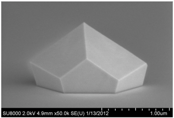 |
| Figure 2: Perfectly faceted GaAs crystallite epitaxial on Si by the ELO technique (C2N image). |
Perovskite/CIGS multijunction
Copper-Indium-Gallium-Sulfur/Selenium cells have demonstrated efficiencies and industrial manufacturing that make them competitive with Si. However, as with Si, the high efficiency achieved (>23%) invites new approaches to achieve significantly higher efficiencies. A tandem structure combining CIGS and Si is the route of choice.
This work is continuing in the framework of the European PERCISTAND project (https://percistand.eu/en), which brings together six European countries and Australia. PERCISTAND is already able to demonstrate cells with a certified efficiency of 25%. The target efficiency is over 30% for a tandem, and over 25% for a module.
Perovskite/Si multijunction
Perovskites are a new class of materials in photovoltaics that appeared about ten years ago. This class has made it possible to achieve efficiencies close to those of Si cells, with very low material costs and simple manufacturing.
This still young field is currently limited by the stability of the perovskite layers which can be degraded under illumination and by chemical degradation due, in particular, to ambient humidity. However, the ease of fabrication of these materials makes their deposition on Si possible, paving the way for a high efficiency Si-based tandem.
This is combined with a new concept, which is the three-terminal tandem solar cell with band offset barrier (3T-SBOB, Djebbour et al., http://dx.doi.org/10.1002/pip.3096). This novel concept in the photovoltaic world, patented in 2017 (https://hal.archives-ouvertes.fr/hal-01420613), allows for tandem solar cell efficiencies without the need for a tunnel junction, or series current continuity. This concept requires the use of a low gap Si cell with interdigitated backside contacts (IBC).
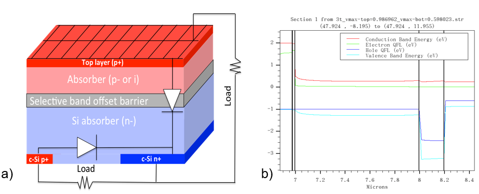 |
| Figure 3: 3T-SBOB tandem cell (THESIS and BOBTANDEM projects) showing (a) the layer stacking and equivalent scheme and (b) the band structure at the interface between the high-gap PSC cell and the low-gap Si-IBC cell, at the maximum operating point of the two sub-cells |