
PV materials and devices
![]()
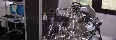
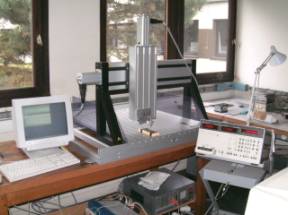
The optimisation of absorber materials, interfaces and devices is the main subject of study in which we participate due to our expertise in electrical and optoelectronic characterisation. Our techniques based on photocurrent, luminescence, admittance, and conductive tip AFM microscopy lead us to collaborate with other laboratories, institutes and industry through national and international projects.
Note that the complexity of the materials and associated devices (multispectral, nanostructured, etc.) has also led us to develop a modelling activity. This activity is based on optoelectronic characterisation and aims to improve the understanding of the physics around the device.
The "PV materials and devices" activity is divided into three thematic areas:
i) silicon and its devices
This research area focuses on silicon-based photovoltaic technologies, and more specifically on the problem of selective passivated contacts. Our studies specifically focus on solar cells with :
- hétérojonction (HET) et son interface a-Si:H/c-Si
- homojonction (HJ) avec une interface poly-Si/SiOx/c-Si
ii) new materials
This area focuses on new absorber materials such as perovskites or indium/gallium-free Zn-IV-N2 alloys.
iii) les structures à multijonctions
The focus is on multijunctions in a tandem configuration (III-V/c-Si, perovskite/CIGS, perovskite/c-Si) and for different types of interconnections (2T and 3T).